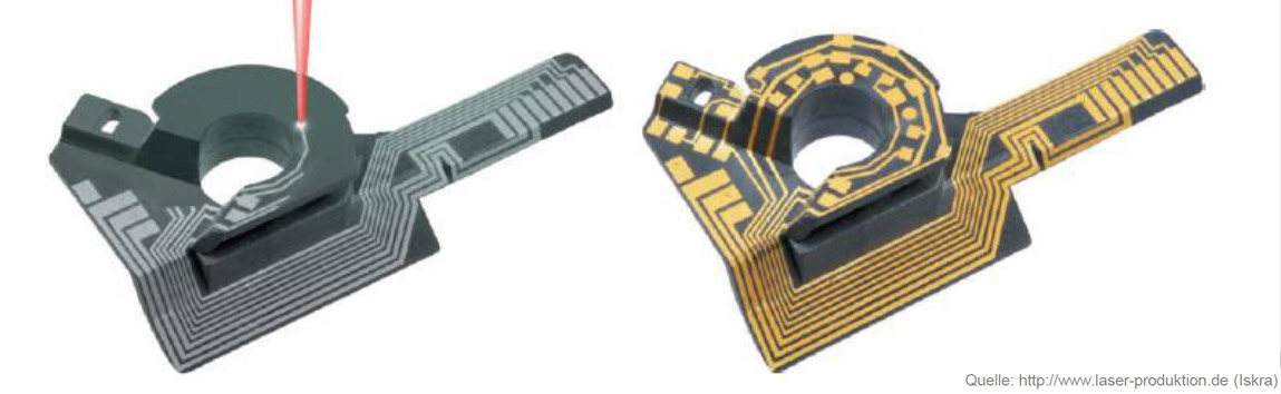
Laser-Direct-Structuring (LDS)
Selective plating of injection molded components by laser-direct-structuring in only three process steps.
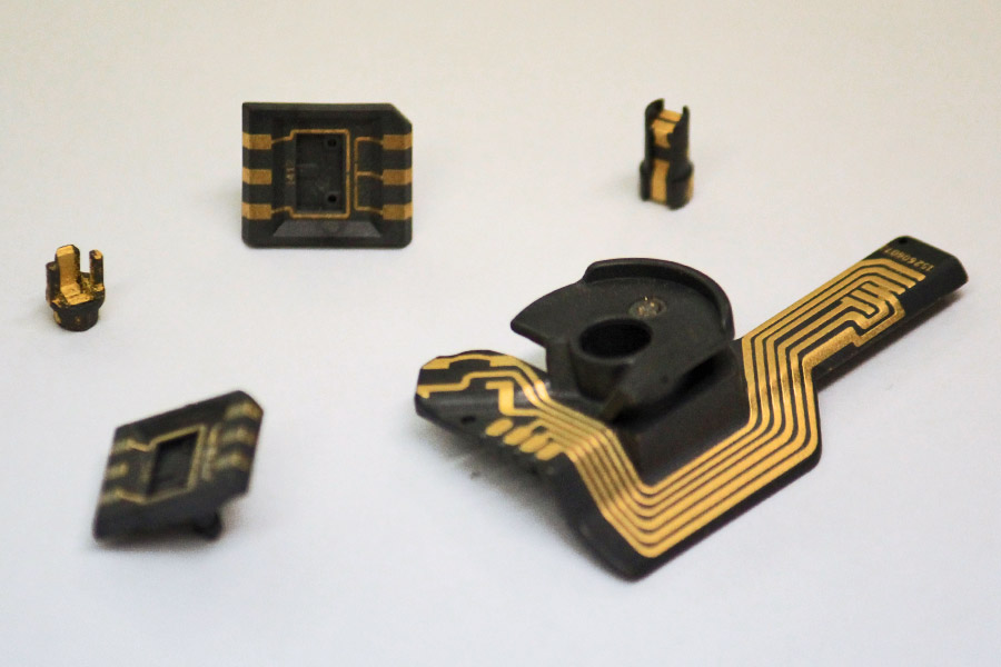
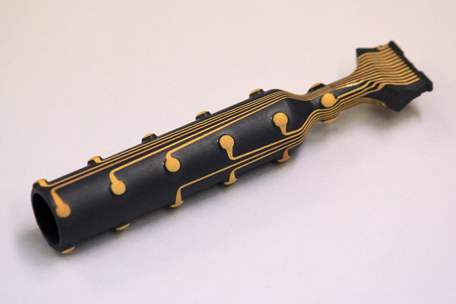
Fields of Application
- Telecommunication
- Antenna technology
- Office technology / data systems technology
- Automotive industry
- Plug-in connector industry
Plastic-Combinations
- ABS = acrylonitrile-butadiene-styrene
- LCP = liquid crystal polymer
- PBT = polybutylene terephthalate (cross-linked by irradiation)
- PPA = polyphthalamide
- PEI = polyetherimide
- PA = polyamide
- PC = polycarbonate
Dimensions
- Minimum PCB-track width 100 µm
(up to 50 μm is possible with a new laser)


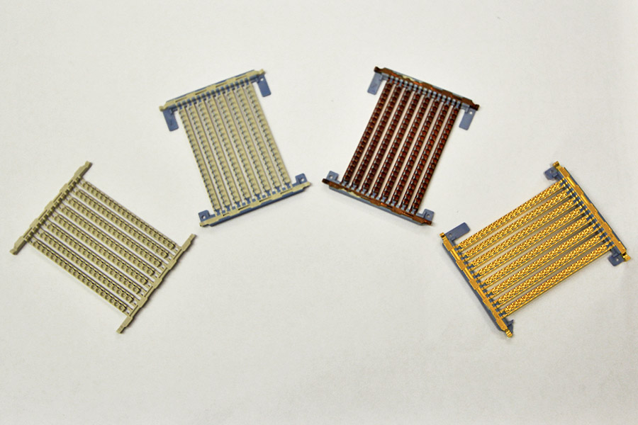

Advantages
- Low tool costs
- Quick layout changes are possible
- Very fine structures are possible
- Parts are solderable
Disadvantages
- Only 2.5-D is possible
- Longer plating process
- Only high temperature resistant materials are applicable
Additive-Procedure
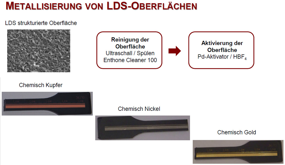
- Complete plating with electroless copper
- Laser structuring
- Contacting the layout surfaces – galvanized enhancement to 20-30 µm
- Differential etching (removal of the electroless copper layer)
- Final surface e.g. electroless nickel/gold
Subtractive-Process
- Complete plating with electroless copper
- Complete plating with galvanized copper and galvanized tin
- Laser structuring (only removes the tin layer)
- Copper etching
- Tin stripping
- Final surface e.g. electroless nickel/gold